


Can additive manufacturing deliver for electronics?
Electronics manufacturing is inherently wasteful, relying on subtractive processes that consume significant amounts of materials and chemicals. For example, during printed circuit board metallisation (PCB), etchants remove large volumes of copper to create the desired circuit patterns, removing most of the original copper as waste. Additive manufacturing offers a compelling alternative by depositing conductive traces only where they are needed, reducing material consumption.
IDTechEx's report ‘Sustainable Electronics and Semiconductor Manufacturing 2027-2037: Markets, Technologies, Forecasts’ outlines opportunities and challenges for players aiming to minimise environmental impacts of electronics. It also explores how supply chain resilience is driving interest in sustainable electronics, amid growing challenges from geopolitical tensions, climate related disruptions, and rising AI driven demand.
The sustainability case for electronics manufacturing is becoming increasingly important as demand for energy, materials, and water continues to grow. Furthermore, global e-waste production volumes are expected to exceed 96 million tonnes by 2037. Additive manufacturing presents a promising route toward more resource efficient electronics production, although significant technical and commercial challenges remain.
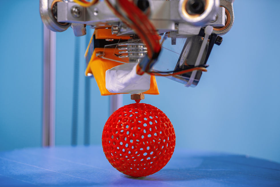
Additive manufacturing offers a more sustainable alternative to conventional electronics production by placing conductive materials only where they are needed. Traditional PCB manufacturing relies on copper clad laminates, photoresists, and chemical etchants such as ammoniacal, ferric chloride, and cupric chloride solutions, generating significant volumes of corrosive acidic and alkaline waste whilst requiring large amounts of water for rinsing. Additive approaches such as printed electronics can significantly lower environmental impact. Estimates have suggested emissions reductions of around 80% and water savings of up to 95% compared with conventional metallisation approaches.
Adopting a new additive manufacturing process can create further sustainability and cost benefits beyond material efficiency, as it provides an opportunity to redesign manufacturing flows from scratch. For example, it may be possible to switch from higher-cost substrates such as polyimide to lower cost alternatives like PET. Additive processes can also enable lower temperature manufacturing, which cuts both energy consumption and operational costs.
While sustainability is a compelling advantage of additive manufacturing, it is not enough on its own to drive widespread adoption. Interviews conducted by IDTechEx indicate strong interest from European and US customers in more sustainable manufacturing processes and products, but this interest rarely translates into purchasing decisions unless cost parity can be achieved. Although adopting an additive process provides an opportunity to redesign manufacturing, it also requires significant capital investment. This presents a major challenge, as conventional electronics manufacturing is already highly optimised, with established infrastructure.
Yield and scale remain significant challenges for additive electronics. Many additive processes struggle to achieve the high yields demanded by cost sensitive electronics markets, while manufacturing complex multilayer devices can be more difficult than with conventional techniques. As one printed electronics company told IDTechEx, its current yield is around 75%, but achieving cost competitiveness will require yields closer to the ~96% typically seen in established subtractive manufacturing. Combined with the economies of scale already achieved by conventional electronics production, this creates a substantial barrier to adoption.
Additive manufacturing is also not the only route to improving sustainability in electronics production. Conventional subtractive manufacturing becomes more efficient through approaches such as etchant regeneration, which reduces chemical consumption and waste generation. In addition, companies such as DP Patterning are developing novel processes, including etchant-free subtractive metallisation of flexible PCBs.
In the near term, additive electronics manufacturing is most likely to gain traction in applications with relatively simple circuit requirements, where flexibility, customization, or sustainability provide clear advantages. Examples include RFID tags for smart packaging, wearable devices and e-textiles that require electronics to be printed onto flexible substrates, and disposable sensors or medical patches where low material use and lightweight form factors are priorities. Additive manufacturing is also well suited to rapid prototyping and low volume production, where eliminating tooling and enabling faster design iterations can deliver value. By contrast, competing with conventional manufacturing in high volume, multilayer consumer electronics will remain challenging in the short to medium term.
To find out more about methods to improve the sustainability, material, and energy efficiency of PCB manufacturing, see ‘Sustainable Electronics and Semiconductor Manufacturing 2027-2037: Markets, Technologies, Forecasts’. The report also covers opportunities to improve the sustainability of semiconductor manufacturing, which currently uses almost 200 billion kWh of energy and 1000 billion litres of water annually.



Comments